Edit this paragraph, high-speed PCB design process traditional PCB design flow, the signal rate is getting higher and higher, even the GHZ above the field of high-speed PCB design is no longer applicable. High-speed PCB design must be the perfect combination of simulation and verification. The simulation is not the traditional sense of a simple design verification, but embedded throughout the design process before the simulation rules, rules-driven design, to the end of the post-simulation
PCB Design Considerations (1) to avoid signal lines, such as clock and reset signals arranged in the PCB edge.
(2) chassis ground and signal lines are separated by at least 4 mm; to keep the chassis ground of the aspect ratio less than 5:1 to reduce the inductance.
(3) has identified the location of the device and line LOCK function to lock it, so that does not malfunction.
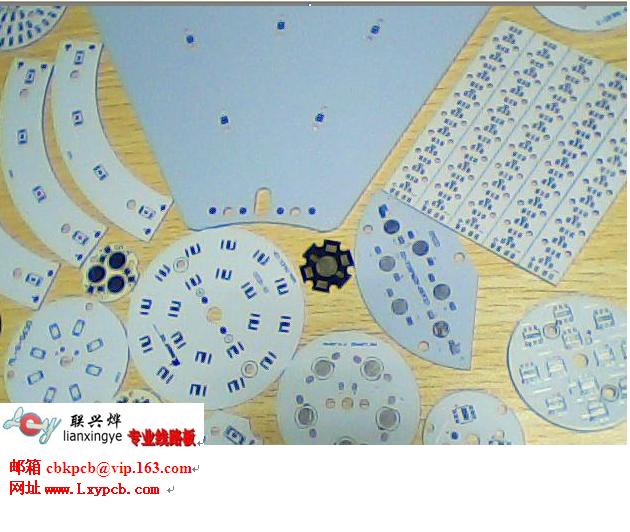
(4) The minimum conductor width of not less than 0.2mm (8mil) in high-density high-precision printed circuit conductor width and spacing is generally preferable to 12mil.
(5) alignment between IC pin DIP package can be applied to the 10-10 and 12-12 principle, that is, when the feet by two lines, the pad diameter can be set to 50mil, line width and line distance are 10mil, when only by a line between the feet, the pad diameter can be set to 64mil, line width and line spacing for 12mil.
(6) In order to increase the pad when the pad diameter is 1.5mm, peel strength, can be long is not less than 1.5mm, width 1.5mm and long circular pad.
(7) Design encounter traces smaller pad connection, the connection between the design you want to pad alignment into a teardrop shape, so that the pad is not easy from the skin, lines and pads is not easy to disconnect.
(8) a large area of copper, copper design should be open window, plus cooling holes, and the window is designed to mesh.
(9) as short as possible to the connection between the high-frequency components, reducing their distribution parameters and the mutual electromagnetic interference. Susceptible to interference components can not endure each other too close to the input and output components should be kept away.
Edit this paragraph, component placement, the connection between the high-frequency components: high-frequency components, the shorter the better, try to reduce the connection of distributed parameter and the electromagnetic interference between the components susceptible to interference can not be too near. The distance between the part of input and output part of the components should be as large as possible.
2, has a high potential difference components: Increase the distance between the high potential difference components and connections to avoid accidental short circuit occurs, damage to components. 2000V potential difference between the copper film from the line in order to avoid the occurrence of creepage phenomenon, general requirements should be larger than 2mm, a higher potential difference, the distance should also increase. Devices with high voltage, you should try to layout of the reach of hand when debugging.
Much weight components: Such components should have a bracket, while the big, heavy, fat calories and more components, and should not be installed on the circuit board.
4, heat and thermal components: Note that the heating elements should be kept away from the thermal component.
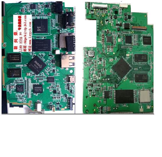
Professional and timely quality integrity-www.lxypcb.com
Address: Industrial Park with the rich industrial Ze Hao, Chun Mei Village, Guangming District, Shenzhen Building A / 516 878 Tel: +86- 0755-89496323 Contact
Luen Hing, Fax 755 -28235433 E-mail: cbkpcb@vip.163.com Lian-Xing Ye Ye Allegro


 2012-06-23